|
Dobrica Pavlinušić's random unstructured stuff
X300 dongle
X300 dongle
JTAGI took picture of both sides of board, corrected it using perspective tool in gimp and added layers with VCC (5V and 3.3V) and GND (checked with unimer continuity test). 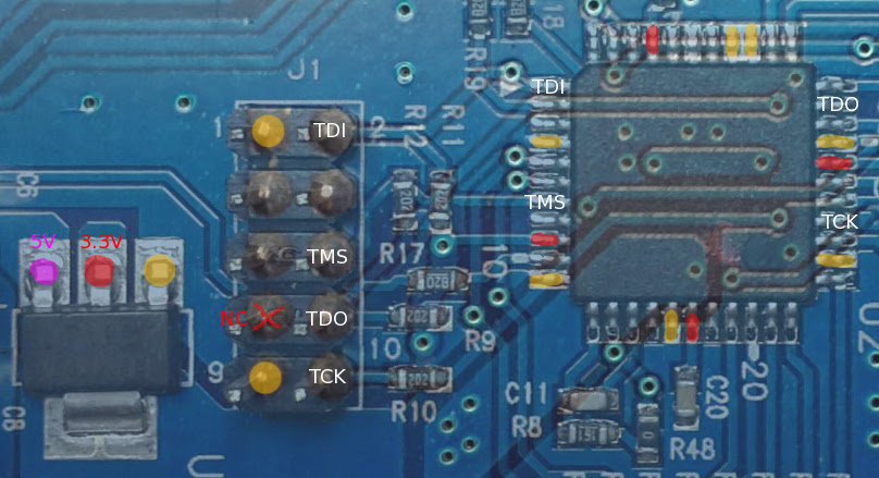 JTAG pinout doesn't match silkscreen designation of pin 1 (it's rotated). It also doesn't have VCC pin connected, so you need to supply 5V power via other means (I used PS/2 connector). Bus Blaster jtag try: jtag> cable jtagkey vid=0x0403 pid=0x6010 interface=0 Connected to libftd2xx driver. jtag> detect IR length: 10 Chain length: 1 Device Id: 00010111000001100100000011011101 (0x170640DD) Manufacturer: Altera (0x0DD) Part(0): EPM3064A (0x7064) Stepping: 1 Filename: /usr/local/share/urjtag/altera/epm3064a/epm3064a jtag> print chain No. Manufacturer Part Stepping Instruction Register ------------------------------------------------------------------------------------------------------------------- * 0 Altera EPM3064A 1 BYPASS BYPASS # IMPORTANT: load signal aliases for this package jtag> include /usr/local/share/urjtag/altera/epm3064a/t44 # get values of all pins jtag> instruction SAMPLE/PRELOAD jtag> shift ir jtag> shift dr jtag> dr 010010111010111010010111010010010010111111111010111010 111010010010010111010010010010010010010010010010010010 010010010010010010010010010010010010010010010010010010 010010010010010111010111010010 (0x0000000000000000000000000000000024924924924975D2) jtag> print chain No. Manufacturer Part Stepping Instruction Register ------------------------------------------------------------------------------------------------------------------- * 0 Altera EPM3064A 1 SAMPLE/PRELOAD BSR jtag> get signal IO2 IO2 = 1 jtag> get signal IO3 IO3 = 1 jtag> get signal IO43 IO43 = 1 jtag> get signal IO44 IO44 = 1 # toggle single pin jtag> instruction EXTEST jtag> shift ir jtag> print chain No. Manufacturer Part Stepping Instruction Register ------------------------------------------------------------------------------------------------------------------- * 0 Altera EPM3064A 1 EXTEST BSR jtag> set signal IO10 out 0 jtag> shift dr # re-read values of all pins jtag> instruction SAMPLE/PRELOAD jtag> shift ir jtag> shift dr jtag> get signal IO10 IO10 = 0 SVF programmingjtag> svf /blue-zfs/FPGA/Altera-x300/x300_dongle/output_files/dongle1.svf stop progress detail: Parsing 20/520 ( 3%)warning: unimplemented mode 'ABSENT' for TRST detail: Parsing 520/520 (100%)detail: detail: Scanned device output matched expected TDO values. VHDL to toggle pinsToggle pins on all four sides of CPLD and create additional two images with all one and all zero for easy test where pin is dongle1.vhdThen I connected logic analyzer on pins and tried different svf files (all-0, all-1, left, bottom, right, top) to locate which pin change depending on image loaded. To isolate pins I used EXTEST and toggled pins. RJ45 
PS2http://www.computer-engineering.org/ps2protocol/
6-pin Mini-DIN (PS/2): Keyboard (left, purple)
Mouse (right, green)
Audio jackR2R D2A all measurements are done on Hantek 2090 with 500mV/div setting which may account for some accuracy errors channel 1
channel 2
|


